")
")
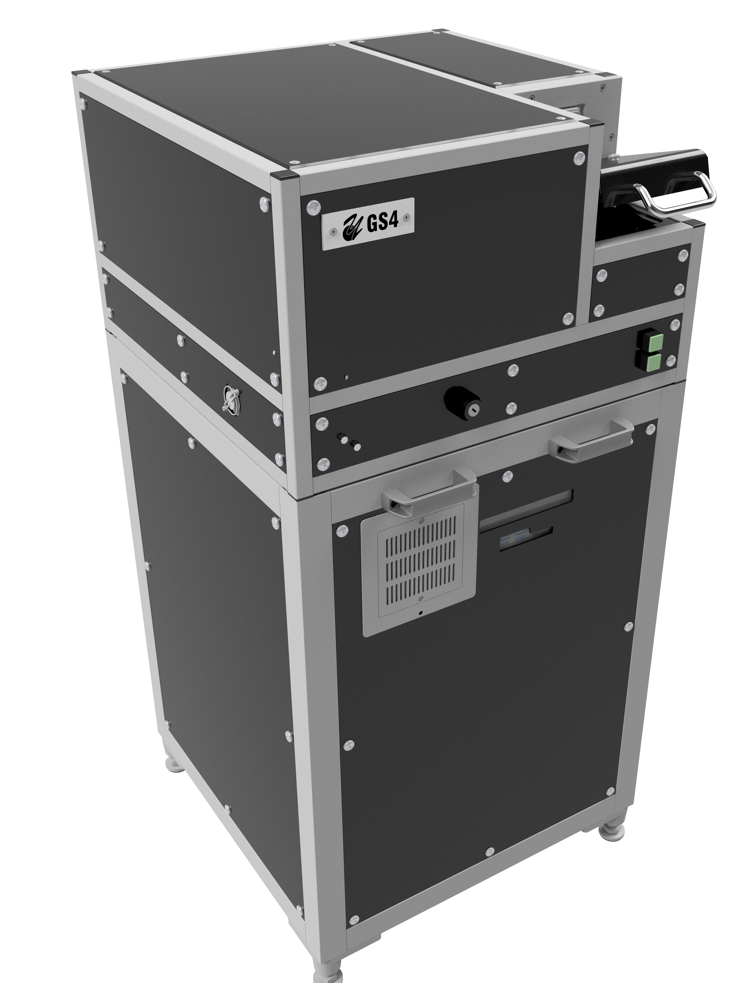
YWafer Mapper GS4
- Parent Category: YWafer Inspector
- AK8
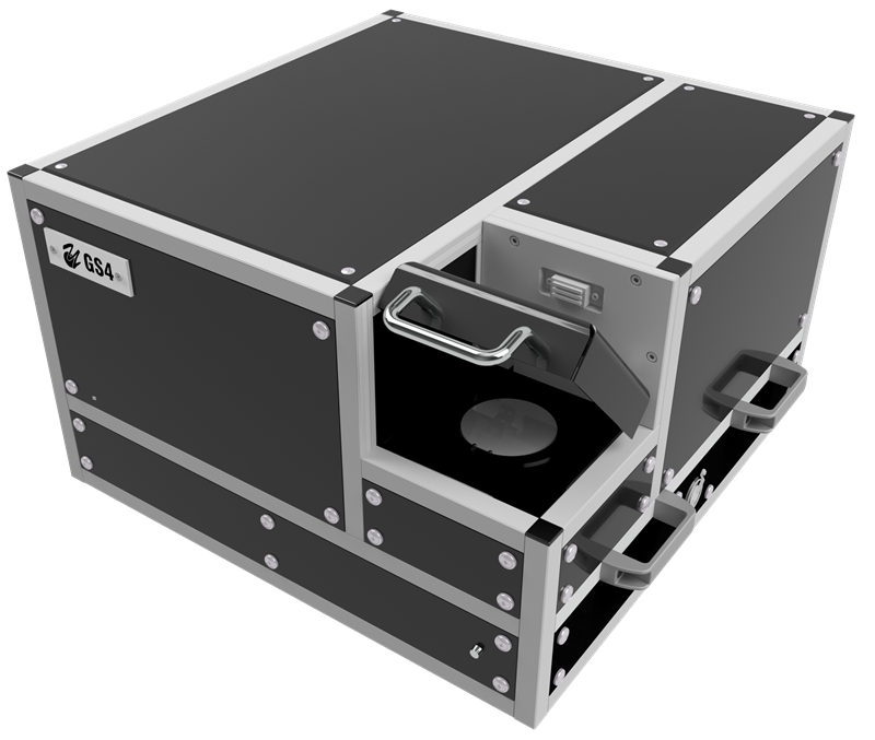
100x100mm area (2 to 4 inch wafer) photoluminescence, epitaxial layer thickness mapping, wafer curvature measurement system and more for LED/LD, sensor materials, phosphors in R&D and production.
Features up to 5 pre-installed photoluminescence laser excitation sources, transmitivity, reflectivity measurement in one extremely compact design.
YWafer Mapper GS4-WL
- Parent Category: YWafer Inspector
- AK8
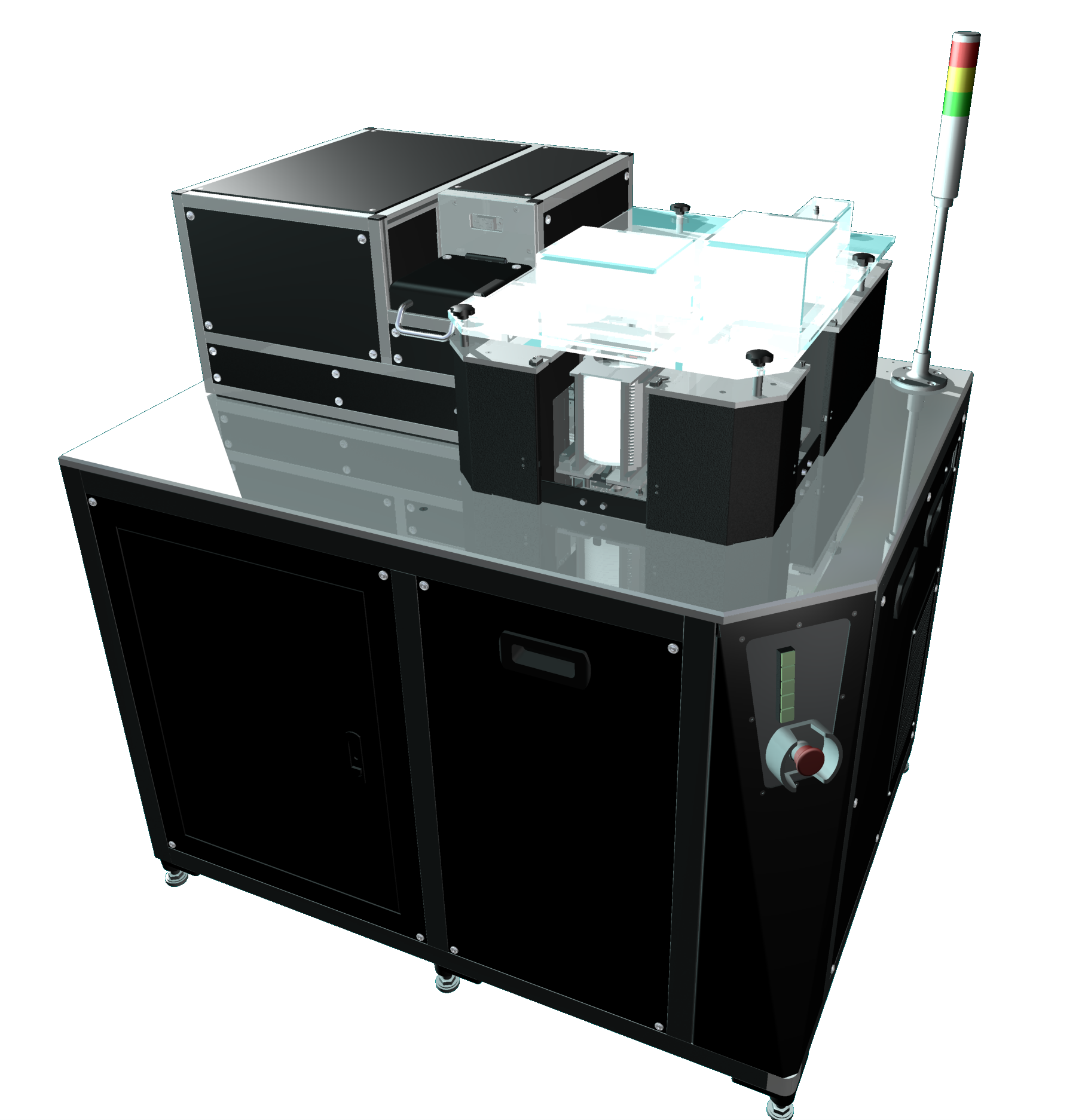
This product has been discontinued. For custom automation of the YWafer Mapper GS4, please contact us.