")
")


![]()
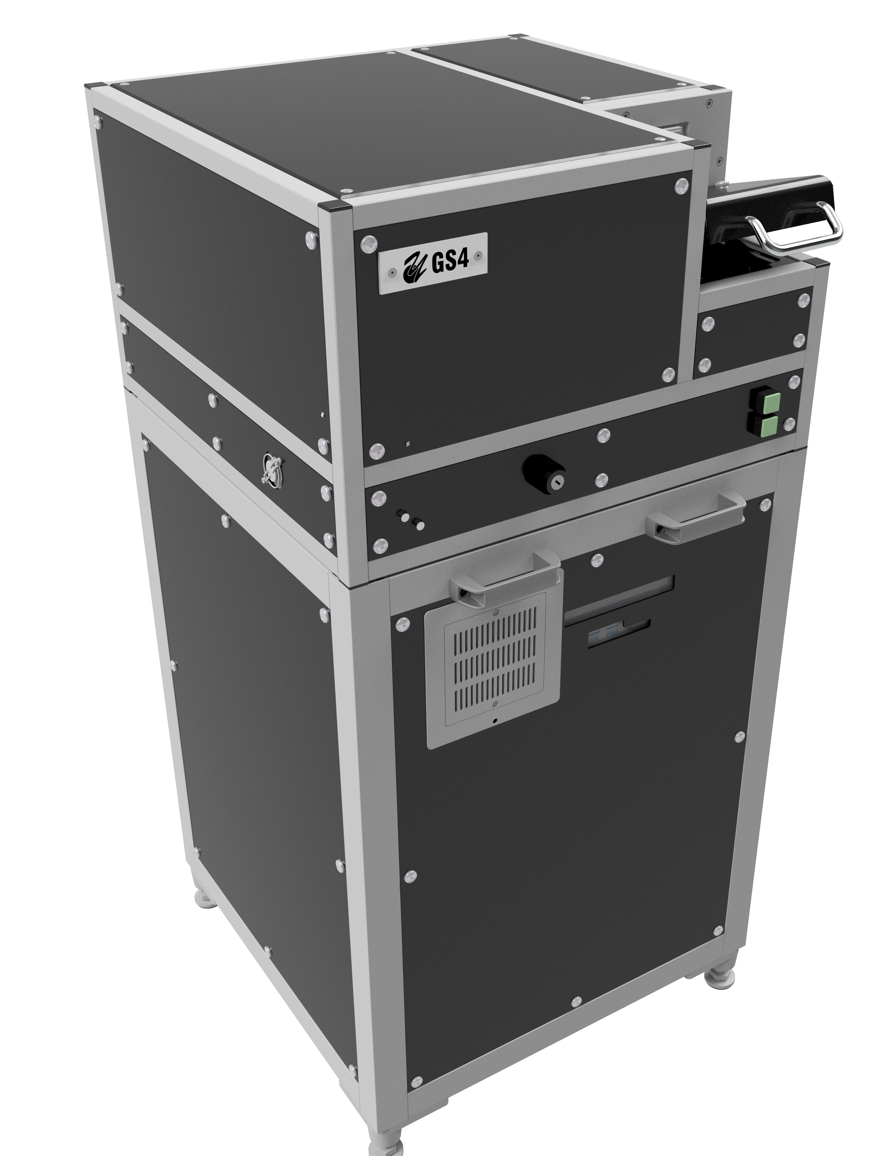
One of our latest models in the YWafer GS4 family of wafer mappers, with a full range of enhanced functions for mapping of photoluminescence, was delivered to Sharp Corporation.
Based on sophisticated optical metrology, the GS4 is more than ever customizable, providing the user with the optimal tool for measuring and mapping GaN-based wafer and more. As its predecessors, the latest version of GS4 is designed to realize rapid, accurate, and highly reproducible measurement across a wide wavelength range and material systems. The GS4 can handle wafer sizes up to 100 x 100mm, and its built-in photoluminescence referencing technology enables the highest possible short and long term measurement stability and reproducibility.
Some possible extensions of the GS4 sysytem include up to 3 laser excitation sources, transmission and/or reflection sources and surface profiling for the measurement of epitaxial thickness, wafer curvature. For more information our mapping products, please follow this link!
ワイ・システムズはDOBOT社との提携により協働ロボットCRシリーズの販売を開始しました!
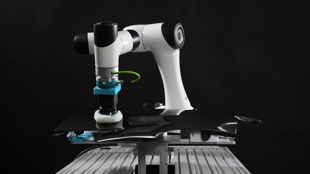
DOBOT 協働ロボットCRシリーズは、3kg、5kg、10kg、16kgまでのペイロードを持つモデルから選択できるコストパフォーマンスの高い6軸ロボットアームです。簡単にセットアップができて、衝突検知、軌道再現などの機能が充実しています。また、直感的で使いやすく、制御しやすいハンドティーチング機能で人間とロボットの協働作業を安全に行えます。
産業用から教育用まで幅広い用途に合わせたシステム設計を含めた販売および技術サポートの提供を開始します。
![]()
One system of our latest wafer mapping product lines, YWafer-RD8, was recently delivered to Toyota Central R&D Labs., Inc. (TCRDL)
Featuring excitation control (for both spot size and attenuation) as well as extremely sensitive detection using both photo-diode and cooled CCD spectroscopy, such a system allows for weak defect band emission measurement over a range of intensities never achieved before.
According to scientists at TCRDL, "We are now able to measure and map the defect emission intensity of our wafers with high sensitivity, over more than 5 orders of magnitude, and moreover, wafer mapping with varying intensities of excitation can be achieved in a fully-automated fashion by using the RD8".
By comparing band-edge emission and defect emission over a large range of excitation conditions it is possible to quantify the quality of the epitaxy, which is critical for the reliability of high power electronic SiC and GaN based device structures.
The RD8 line was designed to do everything that our GS and YB product lines can and more, faster and with a maximum measurement area of 200 x 200mm or up to 8 inch wafers.
See the pesentation by Dr. Lacroix from our booth at the CS Live II conference in November 2020, entitled "Beyond the PL Mapper".
YGM-CRV-1D In Situ Wafer Curvature Monitoring Head
A customized version of YGrowthMonitor (YGM-CRV) for extreme wafer curvature was delivered to a corporation in Japan. Our in situ monitoring products continue to adapt to new needs, in order to provide solutions to an ever growing variety of temperature, stress and reproducibility issues in commercial crystal growth.
![]() 2019 brings new products and featues to our already versatile wafer mapping product line YWafer Mapper.
2019 brings new products and featues to our already versatile wafer mapping product line YWafer Mapper.
YWAFER-GS3 has now been discontinued as 2 to 3 inch wafer mapping is supported by both our GS4 and RD8 models. We will consider supplying GS3's only upon special requests or volume orders. YWAFER-YB products have also merged with the GS and RD series as special configurations of those models.
The current models, separated by mapping area capacity and loading methods is now as follows:
| GS4 | RD8 | -WL26 | -WL48 | |
| up to 4 inch mapping (100x100 mm) | 〇 | 〇 | 〇 | 〇 |
| up to 8 inch mapping (200x200 mm) | 〇 | 〇 | 〇 | |
| 2 to 6 inch robotic wafer loading | 〇 | |||
| 4 to 8 inch robotic wafer loading | 〇 | |||
| over 8 inch mapping or loading | Available as special order | |||
For more detailed information on the various capabilities and configurations that will best suite your needs, please contact us.
Fully automatic wafer mapping system (YWafer GS4-WL) ships to an LED maker in Japan.
YSystems was awarded patent number I 567377 (APPARATUS AND METHOD FOR MEASURING A LUMINISCENT DECAY) by the Taiwan Patent office.
A new production wafer mapping system (YWafer Mapper GS4-WL) for LED fabrication now in operation in Shanghai, China. The system uses all the latest features including high-speed simultaneous mapping of the photoluminescence, epitaxial thickness and surface profile (curvature).
On June 1st, RobotShop Japan opened its online store of robotic products. YSystems and RobotShop Inc. (Canada) joined forces to expand the world leading distributor to include Japan as a logistic center!

Latest high performance GS4 for blue LEDs to be installed at a new LED factory in China. This latest model features simultaneous measurements of eptitaxial thickness, photoluminescence and wafer curvature, a performance to this date only available by YSystems.
![]()
A 200mm measurement area phosphor wafer mapping system, one configuration of our YWafer RD8 lines, has been shipped to the Toshiba Corporate Research & Development Center.
In order to obtain and map characteristics of these materials, our phosphorencence mapping systems (such as our smaller YB3 and YB4) implement a configuration such as used in typical phosphor-based light sources where blue light is partly transmitted from below the wafer, and yellow light is emitted from the absorbed portion. (Click here for more information on the measurement method)
The standard configuration of these systems includes CIE parameterization of the total light emitted at several angles, as well as wafer thickness mapping, and features state of the art measurement reproducibility. Optional interchangeable excitation light sources are also available. Custom wafer adapaters, or other customization can typically be implemented without compromizing the core features of the RD8.
Please contact us for more details about this product.
YWafer YB system ships to a phosphor wafer maker in Japan.