")
")
![]()
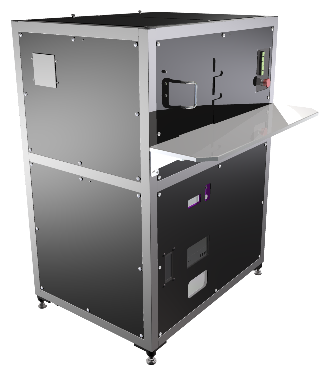
One system of our latest wafer mapping product lines, YWafer-RD8, was recently delivered to Toyota Central R&D Labs., Inc. (TCRDL)
Featuring excitation control (for both spot size and attenuation) as well as extremely sensitive detection using both photo-diode and cooled CCD spectroscopy, such a system allows for weak defect band emission measurement over a range of intensities never achieved before.
According to scientists at TCRDL, "We are now able to measure and map the defect emission intensity of our wafers with high sensitivity, over more than 5 orders of magnitude, and moreover, wafer mapping with varying intensities of excitation can be achieved in a fully-automated fashion by using the RD8".
By comparing band-edge emission and defect emission over a large range of excitation conditions it is possible to quantify the quality of the epitaxy, which is critical for the reliability of high power electronic SiC and GaN based device structures.
The RD8 line was designed to do everything that our GS and YB product lines can and more, faster and with a maximum measurement area of 200 x 200mm or up to 8 inch wafers.